Organisations: 3rd Physics Institute University of Stuttgart, Leibniz-Institutfür Oberflächenmodifizierung, Institute of Physics, University of Augsburg, Element Six, University of Tsukuba, TTI/SQUTEC
Authors: S. Santonocito, A. Denisenko, R. Stöhr, W. Knolle, M. Schreck, M. Markham, J. Isoya and J. Wrachtrup
Publication location: New Journal of Physics, Volume 26
Year (date): 2024
D.O.I: 10.1088/1367-2630/ad2029
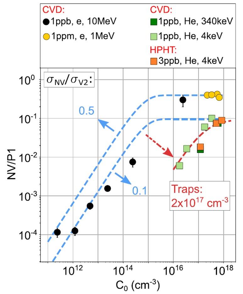
Advances in applications of nitrogen-vacancy (NV) spin centres in diamond for sensing and quantum metrology depend critically on the NV fabrication methods. One such technique combines epitaxial diamond growth and electron or ion irradiation (He, C, etc), where NVs are activated by vacancy trapping at the nitrogen donor atoms upon thermal diffusion. In this work we study the efficiency of such method by analyzing NV depth profiles created by 340 keV and also 4 keV He irradiation in high purity CVD and HPHT diamond crystals and subjected to sequent annealing at 950 ◦C and 1200 ◦C temperatures. This analysis is coupled with the measurement of NV density in the bulk of CVD diamonds with nitrogen doping at low-ppb and low-ppm levels, exposed to MeV electrons in a wide range of the doses. For data analysis we developed an atomistic model based on probabilistic atomic jumps in a crystal lattice, which considers competitive trapping between di-(V2) or multi-vacancy defects compared to that of NVs. The efficiency of NV formation was defined as a ratio of the corresponding capture cross sections: σNV vs. σV2. Applying this model to the experimental data, the σNV/σV2 ratio was estimated about 0.1–0.5, where the activation energy of vacancy diffusion of about 1.7 eV was evaluated by 3D localization of individual NVs in depth profiles in a confocal microscope and sampling their spin coherence properties (T2). In addition, we noted two subsidiary effects also discussed here: (i) reduction of NV density within the stopping range of the implanted He atoms after 1200◦ annealing and, (ii) partial suppression of NVs at near-surface areas visible only at low-dose electron exposures. The results of this study could be helpful to optimize the NV fabrication process reducing the density of ‘collateral’ lattice damage.